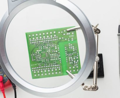

In the world of semiconductor design, RTL to GDSII represents the full lifecycle of transforming a high-level logic description into a physically manufacturable layout. For product companies and fabless startups alike, understanding this process—and having a reliable design services partner—is crucial to achieving first-pass silicon success.
In this guide, we’ll break down the RTL-to-GDSII process step-by-step, explain where outsourcing adds value, and how Nsemi Design ensures quality across the entire flow.
What is RTL to GDSII?
“RTL to GDSII” refers to the back-end VLSI design flow starting from Register Transfer Level (RTL) code (typically in Verilog or VHDL) and ending with the GDSII file used for chip fabrication.
This process includes:
✅ Synthesis
✅ Design for Test (DFT)
✅ Floorplanning
✅ Placement & Clock Tree Synthesis (CTS)
✅ Routing
✅ Static Timing Analysis (STA)
✅ Signoff (LVS, DRC, IR/EM, etc.)
👉 Also Read: VLSI Design Services – What They Are and How to Choose the Right Partner
Key Stages in the RTL to GDSII Flow
1. RTL Handoff and Synthesis
- Input: Clean, synthesizable RTL
- Goal: Convert RTL into a gate-level netlist
- Tools Used: Design Compiler, Genus, Yosys
2. Design for Test (DFT)
- Scan insertion
- Boundary scan, MBIST
- Fault coverage reports
💡 A strong DFT strategy helps avoid costly silicon respins.
3. Floorplanning and Power Planning
- Macro/block placement
- IO planning and pin assignment
- Power grid definition
4. Placement & Clock Tree Synthesis
- Standard cell placement
- CTS to ensure minimal clock skew
- Early congestion analysis
5. Routing
- Global and detailed routing
- Crosstalk, antenna, and signal integrity checks
👉 Dive Deeper: Physical Design in VLSI – Key Steps and Challenges
6. Timing Closure (STA)
- Worst-case path analysis
- Setup/hold violation fixes
- Multi-mode multi-corner (MMMC) optimization
7. Physical Verification and Signoff
- DRC, LVS (Layout vs Schematic)
- IR drop and Electromigration (EM)
- Tape-out-ready GDSII file generation
Where Outsourcing Makes Sense
Handling RTL to GDSII in-house requires large teams and costly tool licenses. Outsourcing to a service company like Nsemi Design gives you:
- Access to EDA tools without added investment
- Expert engineers who’ve done multiple successful tape-outs
- Scalability during crunch time
- Reduced time-to-market
Case Study Highlight: From RTL to GDSII in 10 Weeks
(Insert a real-life anonymized project where Nsemi handled RTL-to-GDSII for a client, saved 30% time, met PPA goals, and passed all foundry checks on the first attempt.)
Best Practices for Successful RTL to GDSII Projects
- Clean, lint-free RTL as input
- Defined timing, power, and area (PPA) constraints
- Early floorplan reviews with physical-aware design
- Regular design reviews with the client
- Formal verification between RTL and netlist
Why Choose Nsemi Design for RTL to GDSII
At Nsemi, our RTL to GDSII offering includes:
✅ Full toolchain support (Cadence, Synopsys, Mentor)
✅ Engineering teams with 7nm to 65nm experience
✅ Strong documentation, progress tracking, and client communication
✅ Flexible engagement models (project-based, hourly, ODC)
Related Blogs to Explore
- 🔗 VLSI Design Services: What They Are and How to Choose the Right Partner
- 🔗 Physical Design in VLSI: Key Steps, Tools, and Challenges
- 🔗 Top VLSI Companies in India for Design Outsourcing
- 🔗 Why Verification is the Heart of Every VLSI Project
Let’s Build Your Next Chip
Ready to start your next ASIC or SoC project?
✅ Contact Nsemi Design today for a customized RTL to GDSII execution proposal.
🔗 Visit: nsemidesign.com